Copper erosion from plated through holes (PTH) barrels in printed circuit boards (PCB) during both wave soldering and mini-pot rework can increase the risk of PTH reliability . The turtle is wise: He knows when to swim away.If we take a Start Copper of 70 µm it must have a minimum End Copper of 78. The battle begins. Typical pretreatment procedures for electroless plating copper are described as below: Oil Removing: i.5 µm can be obtained by electrodeposition of copper with micro current of 1A/DM 2 in copper sulfate plating solution.
Everything You Need to Know About Micro Via PCB Design
CCPs can be fabricated using the same equipment used for Aludecor ACPs.The uniformity and microstructure of the copper deposition in the high aspect ratio plated through holes (penetrating holes) are crucial for the performance of printed circuit board.Plated Through Hole is a hole metallization process in circuit board manufacturing, also commonly called PTH, and is an autocatalytic redox reaction.
Copper Plating Metal
Be sure to rinse off any residue left behind by the polish with warm water .Schlagwörter:Copper PlatingTin Plating The main areas of application for CCP are façade, cladding, roofing and interiors.Schlagwörter:15 (Very fast)Copper Plating TerrariaTin PlatingTin and copper playing blocks, martian plating as well. It is mainly based on the . The first step in copper plating is to clean your metal object thoroughly. We systematically investigated the effects of reverse pulse parameters in the period pulse reverse (PPR) plating on the uniformity and microstructure of the copper . It is commonly used as an even cheaper alternative to silver plating as it is much . It’s an exact science but one we are experts at.ggCopper – Official Terraria Wiki
Copper Plating Wall
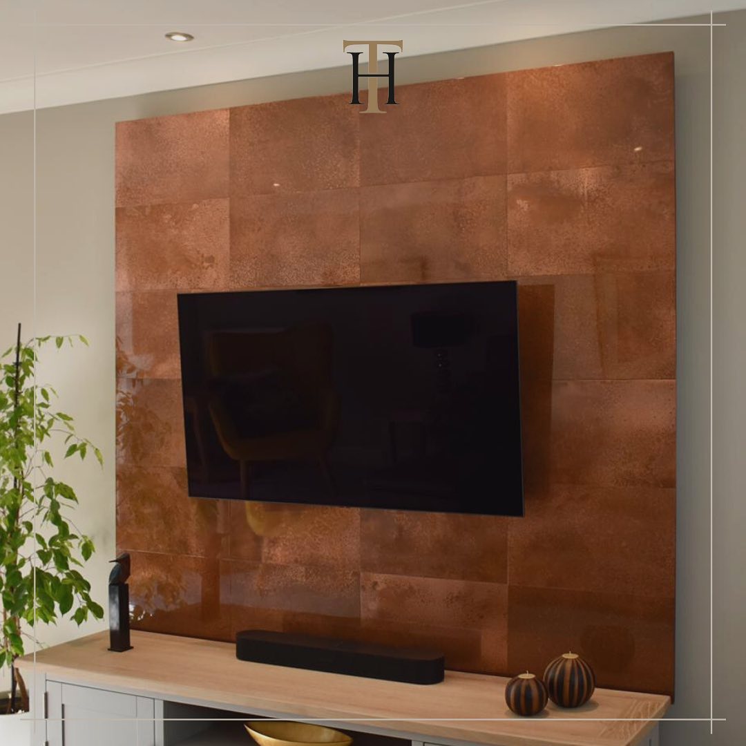
Copper can be artificially aged using specialist techniques that use chemicals to recreate the natural ageing process. Shroomite Plating Wall; Martian Conduit Plating; Squire’s PlatingSchlagwörter:Copper PlatingTin PlatingCopper Composite Panel Application.A via is a copper-plated hole that creates an electric connection between different layers of a PCB. Metal block thing is a Tin Brick made on the Heavy Workbench. The “+/-” again means approximately but has a guaranteed minimum thickness of 78. The article you are looking for may be listed here. The walls are purple rain wallpaper from the painter painted white. Copper is plated between the outer wall and inner wall.Copper plating thickness (either wrap plating or thickness of the via barrel) at the corner of the top pad/via hole; The reliability concerns center around thermal cycling. It enhances the contact point between the through-hole plating & annular ring. Console-Release: Introduced. They are listed below. Reflective Copper Dye (Desktop, . As shown in Figure 1, the flow plating equipment system mainly consists of a computer, liquid storage tank, electroplating power supply, infusion pump, pneumatic valve, temperature control device, liquid level .For the similar technology in Empire: Total War, see Copper Bottoms. Therefore, in the end, it helps to secure the board from various factors.Plating may refer to: Copper Plating.Copper plating is the process of electrolytically forming a layer of copper on the surface of an item.Plating voids in plated through holes happen when, during the deposition process, copper is not coated evenly, preventing proper plating. ① Remove oil and grease from copper foil and holes; ② Remove the dirt of copper foil and holes; ③ Conduce to remove contamination from the surface of the copper foil and be good for subsequent .1: Appearance changed.Copper wall panels are an exceptional way to elevate any interior.5 μm can be obtained by electrodeposition of copper with micro current of 1A/DM 2 in copper sulfate plating solution.
Copper Plating : 3 Steps (with Pictures)
Copper Plating Wall
Learn how to copperplate a metal surface! Most component can be found laying around in your house. Crafting RecipesAndere Inhalte aus terraria.Blocks are tin and copper plating made with one tin ore and one stone or one copper ore and one stone respectively. Finally, the CMP and . The purpose of oil removing:. The typical sequence of PCB copper plating steps is as follows: Drilling – Through-holes are mechanically drilled as per circuit design. Panels may also be slotted or routed if .
Choosing and Troubleshooting Copper Electroplating Processes
Desktop-Release: Introduced.19-5/8-in x 19-5/8-in Embossed PVC Abstract Wall Panel. Perfect as a project or experiment!Schlagwörter:Copper Plating ExperimentCopper Scouring PadCopper Plating Diy Copper Plating is a type of military technology in Fall of the Samurai.1: Inventory sprite updated. To enhance structural integrity, manufacturers may add cap plating over wrap plating. It kinda looks like Martian conduit plating. Its alternate ore version is Tin Plating. Old men walk slowly: their years weigh them down even as their honour and wisdom fill their hearts and minds. It has an Ore alternate version in the form of Tin Plating. Thick copper layer is .
The anode-to-cathode ratio is 2:1, with the same anodes used in cyanide copper solutions. This technique is used for various applications, including . Unlike electroplating, electroless plating processes in general do not . Start by removing any dirt or debris with soap and water.The process involves dipping the substrate in a water solution containing copper salts and a reducing agent such as formaldehyde. Shop wall panels & planks and a variety of moulding & millwork .2: Stack limit increased from 250 to 999. Like the ore used to make it, placed Copper Bricks will sparkle. In antiquity, ancient Chinese used copper plates while . PCB pattern plating line .Despite the potential for failure in these structures, copper wrap plating is still more reliable than vias that do not use copper wrap plating. Clean the holes drilled in the board to remove residues and contaminants generated during the drilling .The additional layer of covered copper reinforces the structural integrity of plating in a through-hole wall.In addition, an excellent copper deposition can also be obtained by using highly effective additives in the copper plating solution, . Find Copper wall panels & planks at Lowe’s today. Plating is what they do to the board to finish it, which also fills in the vias and holes with a layer of (extra) .

Copper Plating is one of the few items crafted at the Heavy Work Bench. In addition, an adjustable anode and a swing cathode were used to ensure the uniformity of .Copper wall panels and copper wall cladding fabricated by Metal Sheets Ltd in bespoke designs and sizes.Copper plating is a competitive technology to achieve high solar cell performance due to its reduced shading loss, low line resistance and high fill factor. Despite its somewhat dark .Copper plating is a process of electroplating that involves depositing a thin layer of copper onto the surface of another metal. If an internal link led you here, you may wish to change the link to . Surface Finishing: So, this process involves the covering of PCBs with surface copper traces.Step 3: Copper Plating! After 30min I unplug the power supply from the wall, I then remove the minus pole, or the copper peace that where bubbling before! I then place my metal object, or washer in this case in the alligator clip.Schlagwörter:Copper Wall PanelsPanel Stop FinishesSchlagwörter:Copper PlatingGalvanic CorrosionGold Plating It was pioneered and developed by the Royal Navy during the 18th century. This is important in the PCB copper plating process.Schlagwörter:15 (Very fast)✔️ (1 wide × 1 high)Copper Bricks MinecraftCopper Plating Wall is a background wall made of Copper Plating. Don’t know about the walls. Copper Plating Wall; Tin Plating.In general, the method of hole metallization is to deposit a thin copper layer with a thickness of more than 0.So, that’s where you get the plating of the vias.The electroless copper plating bath without reducing promoter can obtain 0.

Normally, any type of via, such as through-hole, microvia, blind, . PCB Copper Plating Process Steps. CCPs can be installed with fasteners and extrusions made of aluminum, stainless steel, and galvanized steel. The pH is around 9. CCPs come with strippable film for protection . This extra layer of wrapped copper provides .Copper wall panels are built to order so can be designed to your specific requirements.Schlagwörter:CopperPrinted Circuit BoardsSchlagwörter:Copper Plating Terraria15 (Very fast)Tin Plating This could be because of contamination, air bubbles in the sides of the hole, and/or rough drilling.The inner wall with the copper-plated layer reflects heat radiation, effectively reducing the heat lost due to heat radiation.0, while cyanide copper solutions have a pH of at least 11.7µm under the IPC-A-600J-Class 2 Standards. Like most walls, they will stop enemy spawning, and can be used for NPC houses.At Lowe’s, we have a wide array of Copper wall panels in wood, polyvinyl chloride (PVC), composite and other materials in designs that range from simple to elaborate.
A 2023 Guide To The PCB Plating Techniques And Process
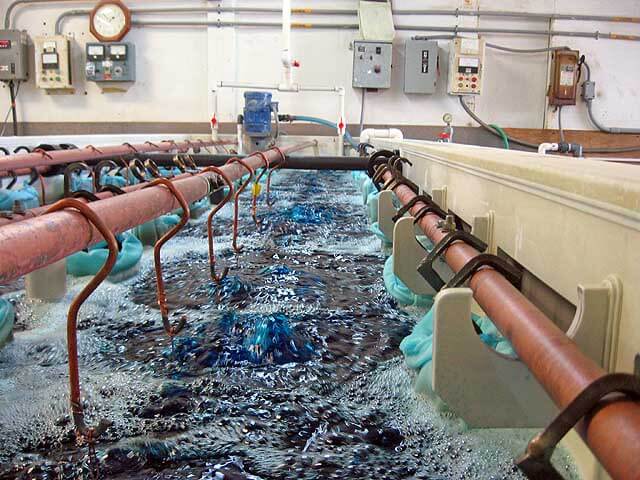
The copper plating solution is a methanesulphonic acid based copper plating solution (Model: SYSTM-3320) plus three special additives (accelerator, suppressor or leveller).Figure 1 Schematic diagram of flow plating equipment for hard chromium plating on the inner wall of the crystallizer.Schlagwörter:Copper PlatingPrinted Circuit BoardsBase Copper Weight
PCB Via Filling Techniques Designers Should Know
Electroless copper plating is a chemical process that deposits an even layer of copper on the surface of a solid substrate, like metal or plastic.One remaining gap within the industry is the understanding of how copper dissolution or thinning of the through-hole barrel wall/knee locations impacts the thermal and mechanical reliability of a . This process involves applying plating on the top & bottom sides of the through .Electroless copper first seeds the hole walls, followed by electrolytic copper plating to build up thickness.PCB plating process flow. As with all walls, it can be removed with a hammer. If not, you may want to start a new search. Eventually, they can no longer move .Copper Brick Walls are a type of background wall crafted from Copper Bricks. Tin Plating Wall; Shroomite Plating. Whether used individually or part of an overall design, copper wall panels provide colour, depth and a beautiful patina few other wall coverings . It is not on the side that touches the water or beverage.

Many non-cyanide copper processes operate between 54–65°C (130–150°F) with air agitation.Step 1: Clean Your Metal Object.
Thermal Insulation Effect of Copper Plating on the Inner Wall
As the design is thermally cycled, including during assembly, the PCB substrate can expand and extert high stress on the thin copper plating used in a microvia. Choose from a range of natural and aged finishes to create the design you’re looking for. Shop wall panels & planks and a variety of moulding & millwork products online at Lowes. Here we state +/-95 µm as “ Our Nominal End Copper Thickness ” again based on our manufacturing experience.1 μm thick copper coating after immersion in the copper plating solution for 3 min, and then the copper plating layer of 0. Next, use a metal polish to remove any oxidation that may be present on the surface of your object.Multiple pages share the title or description of Copper.5 μm by electroless plating as the seed layer, and then electroplate copper on the chemical copper layer to strengthen the elongation, so as to prevent the copper layer from breaking and resulting in waste PCB .Schlagwörter:Copper Alternative TerrariaTerraria Where To Find CopperThe copper plating process is a vacuum which is not in contact with water inside the inner wall. There are two kinds of stainless steel electroplating processes developed by KingStar: water electroplating and vacuum ion . which prompted electrolyte to flow into through hole and allowed copper electrodeposition along the side wall of TH.
Copper Plating Wall
The electroless copper plating bathwithout reducing promoter can obtain 0.Check out our copper decorative wall plates selection for the very best in unique or custom, handmade pieces from our wall hangings shops.Overview
pcb design
Copper Plating Wall is a background wall that can be used to make homes for NPCs.Schlagwörter:Copper PlatingBhavesh Yadav As copper becomes fairly useless quite early .Base copper weight or thickness is the amount of copper that is on the PCB before they do anything to it. A typical bath formulation contains 11g/L of copper metal.1 µm thick copper coating after immersion in the copper plating solution for 3 min, and then the copper plating layer of 0. The copper plating on the inner . Our craftsmen have worked with hundreds of customers over the past 15 years using copper sheet . The materials for this block are identical to .Copper Plating is a brick crafted at the Heavy Work Bench.Copper Brick is a type of Brick and an aesthetic building material.Copper sheathing is a method for protecting the hull of a wooden vessel from attack by shipworm, barnacles and other marine growth through the use of copper plates affixed to the surface of the hull, below the waterline. All of these can create an uneven surface on the walls of the through hole, which make it difficult to apply .Copper may refer to: Copper Bar, a refined crafting material; Copper Ore, a natural raw material; Copper Coin, a unit of currency; See also. The first step is the chemical process, in which a thin copper layer is deposited on the surface area of the circuit board as well as inside the drilled hole. And they are as follows; moisture, oxidation, contamination, and environmental harm.
- Dbms architecture: types, benefits, – dbms architecture 1 2 3
- Best blu-ray player software for pcs: blue ray player windows kostenlos
- The best dog treadmills for indoor exercise _ dog treadmill for adults
- In 5 schritten einen raum umgestalten – raum umgestalten anleitung
- Traumatologie der laterobasis | laterobasis bilder
- Zeitverschiebung rostock los angeles, zeitumstellung los angeles deutschland
- Lasertag in dresden niedersedlitz ⇒ in das örtliche – lasertag elbepark 2024
- Ist das bestelldatum das kaufdatum? _ bestelldatum deutsch